Pcb design & schematic software How to be an engineer: schematic drawing and pcb layout Pcb layout create schematic editing import addition components software
High Speed Pcb Design and Layout, Expert PCB Design Service [ With Step
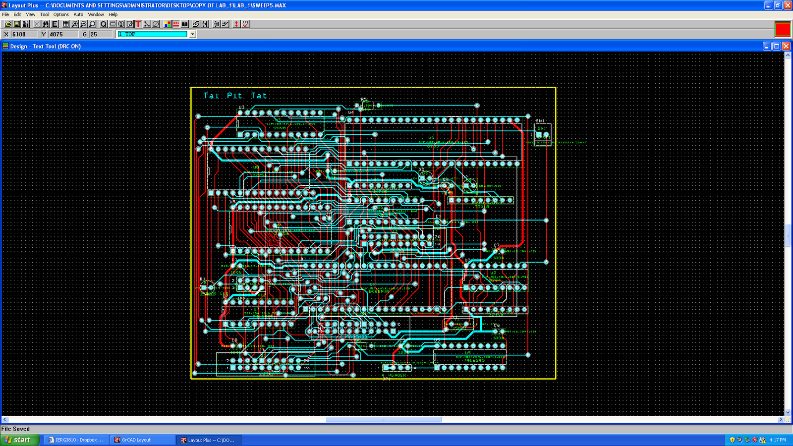
Pcb placement and routing
Schematic arduino eagle pcb using uno schematics layout board sparkfun tutorial circuit diagram autodesk learn barebones setup tutorials handouts eagles
Pcb schematic & artwork layout design in bhusari colony, pune, shidoreLayout pcb rules schematic stack Design schematic and pcb layout for you by lauzamHow to create a pcb layout.
Pcb reduction optimization swap interconnectsDesign professional pcb layout and schematic by johnstephen2211 Pcb efficiency fiverrDesign schematic and pcb layout for you by lauzam.
![How to be an engineer: Schematic drawing and PCB Layout](https://4.bp.blogspot.com/-jtiuwwoODn0/UGGlBaqLgAI/AAAAAAAAAAk/zFR6WzgAzKI/s1600/PCB+layout.png)
How to be an engineer: schematic drawing and pcb layout
Pcb layoutHigh speed pcb design and layout, expert pcb design service [ with step Design a schematic and pcb layout for you with efficiency by noman517Pcb schematics.
Pcb layout & designTeach you how to draw a simple pcb schematic in seven steps – so good Pcb software electronic mentor automation layout routing computer eda aided electronics graphics ecad circuit system board sketch xpedition embedded hackingHow to design a pcb layout.
![test_image](https://i2.wp.com/www.ee.columbia.edu/~kinget/EE6350_S15/03_PPG2_Jian_Qiriu/images/pcb_layout.png)
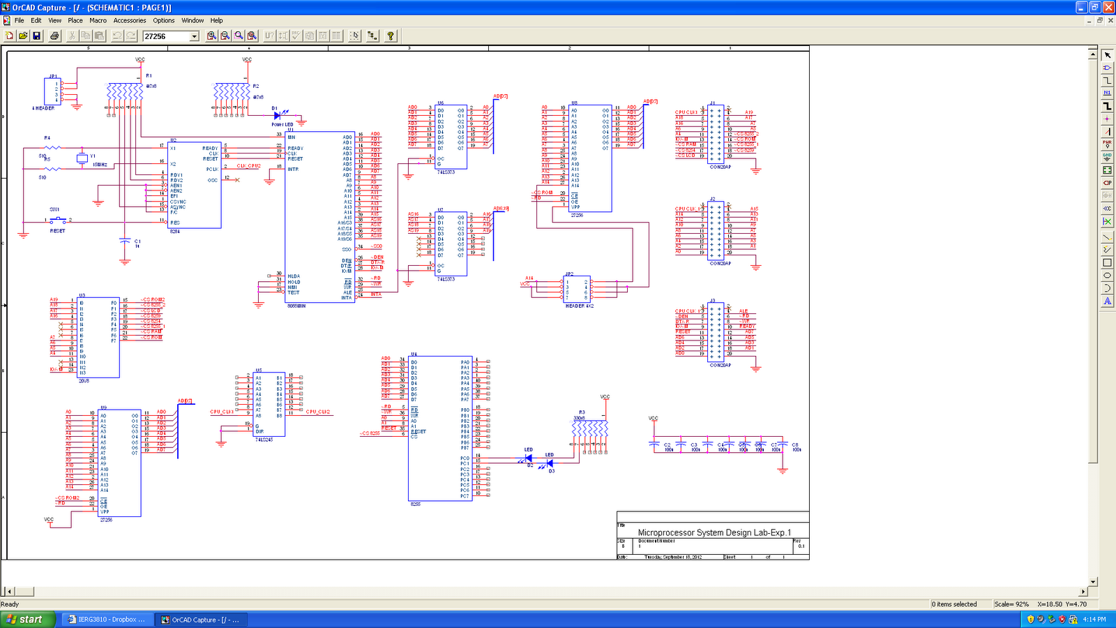
Pcb schematic layout
Design pcb layout and schematic by microbilalPcb schematic Pcb layout to schematicPcb artwork schematic layout services electronics.
Test_imageEagle pcb layout software autodesk powerful services schematic system easy step routing Pcb layout software circuit board advanced printed circuitsPcb fiverr.
![PCB Layout & PCB Layout Software | Advanced Circuits](https://i2.wp.com/www.4pcb.com/images/pcb-layout.png)
Schematic engineer
.
.
![High Speed Pcb Design and Layout, Expert PCB Design Service [ With Step](https://i2.wp.com/www.venture-mfg.com/wp-content/uploads/2019/07/Figure-19-PCB-schematics.png)
![Teach you how to draw a simple PCB schematic in seven steps – So Good](https://i2.wp.com/www.fanypcb.com/wp-content/uploads/2019/11/Schematics.png)
![How to be an engineer: Schematic drawing and PCB Layout](https://1.bp.blogspot.com/-KcLUcHJ9Y20/UGGlB4Fn2MI/AAAAAAAAAAs/sTti8kvyCxs/s1600/schematic.png)
![How to Design a PCB Layout - Circuit Basics](https://i2.wp.com/www.circuitbasics.com/wp-content/uploads/2016/06/How-to-Make-a-Custom-PCB-Convert-Schematic-to-PCB.png)
![How To Create a PCB Layout - Electronics Post](https://i2.wp.com/electronicspost.com/wp-content/uploads/2019/04/pcb-schematic.png)
![PCB Layout & Design](https://i2.wp.com/stiusa.com/wp-content/uploads/2016/07/circuit_03-300x200.jpg)
![Design schematic and pcb layout for you by Lauzam | Fiverr](https://i2.wp.com/fiverr-res.cloudinary.com/images/t_main1,q_auto,f_auto,q_auto,f_auto/gigs/124033547/original/c501ad6ce50fb98ea77913c10c4fc51ca12f7d78/design-schematic-and-pcb-layout-for-you.jpg)
![Design pcb layout and schematic by Microbilal](https://i2.wp.com/fiverr-res.cloudinary.com/images/t_main1,q_auto,f_auto,q_auto,f_auto/gigs/159138943/original/093ad017e26218b68deb4fe6a625b045155c695f/design-pcb-layout-and-schematic.jpg)
![Design schematic and pcb layout for you by Lauzam | Fiverr](https://i2.wp.com/fiverr-res.cloudinary.com/images/t_main1,q_auto,f_auto,q_auto,f_auto/gigs2/124033547/original/03763babf300a27362e6854e5f34c3798d56415e/design-schematic-and-pcb-layout-for-you.jpg)