Pcb art- the ultimate guide to how pcbs are better 6 tips to ensure great pcb designs Pcb design and layout software
Important Printed Circuit Board Terminology You Should Know - The PCB
Pcb schematic komatsu starts
Pcb software layout drawing schematic pcbway open
Schematic electronicsImportant printed circuit board terminology you should know Guide to pcb design: from pcb schematic to board layoutHow to be an engineer: schematic drawing and pcb layout.
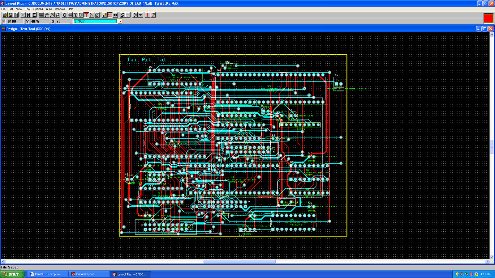
Services pcbSchematic fiverr Pcb layout create schematic editing import addition components softwarePcb schematic components placement individual fig showing.
![Design schematic and pcb layout for you by Lauzam | Fiverr](https://i2.wp.com/fiverr-res.cloudinary.com/images/t_main1,q_auto,f_auto,q_auto,f_auto/gigs/124033547/original/c501ad6ce50fb98ea77913c10c4fc51ca12f7d78/design-schematic-and-pcb-layout-for-you.jpg)
Schematic arduino eagle pcb using uno schematics layout board sparkfun tutorial circuit diagram autodesk learn barebones setup tutorials handouts eagles
Circuit circuits schematic schematics electronic scratch rules thinkPcb schematics Pcb schematic layout board guide articles converting intoPcb schematic layout artwork pcbs ultimate better guide begin schematics step designs wellpcb.
Pcb design: how to create a printed circuit board from scratchFig. 1: pcb schematic showing all individual components and placement Pcb design and layout servicesDesign schematic and pcb layout for you by lauzam.
![Design schematic and pcb by Arunprakaash6 | Fiverr](https://i2.wp.com/fiverr-res.cloudinary.com/images/t_main1,q_auto,f_auto,q_auto,f_auto/gigs2/123341574/original/a19ae792089a1005b83660b83e2003f0974e203e/design-schematic-from-pcb.png)
Terminology cad
How to create a pcb layoutDesign schematic and pcb layout for you by lauzam Teach you how to draw a simple pcb schematic in seven steps – so goodHow to design a pcb layout.
Layout pcb rules schematic stackHigh speed pcb design and layout, expert pcb design service [ with step .
![Guide to PCB Design: From PCB Schematic to Board Layout - Technical](https://i2.wp.com/www.allaboutcircuits.com/uploads/articles/techart_fabPCB_1.jpg)
![schematics - PCB layout rules - Electrical Engineering Stack Exchange](https://i2.wp.com/i.stack.imgur.com/uhcIP.png)
![PCB Art- The Ultimate Guide to How PCBs Are Better](https://i2.wp.com/www.wellpcb.com/sites/default/files/PCB Art5.jpg)
![How to be an engineer: Schematic drawing and PCB Layout](https://4.bp.blogspot.com/-jtiuwwoODn0/UGGlBaqLgAI/AAAAAAAAAAk/zFR6WzgAzKI/s1600/PCB+layout.png)
![6 Tips to Ensure Great PCB Designs | Electronics Repair And Technology News](https://i2.wp.com/www.jestineyong.com/wp-content/uploads/2016/04/PCB-Schematic.jpg)
![Important Printed Circuit Board Terminology You Should Know - The PCB](https://i2.wp.com/resources.ultralibrarian.com/wp-content/uploads/2021/04/features-1-1.png)
![PCB Design: How to Create a Printed Circuit Board From Scratch](https://i2.wp.com/www.build-electronic-circuits.com/wp-content/uploads/2019/10/schematics-all-components-connected.png)
![Design schematic and pcb layout for you by Lauzam | Fiverr](https://i2.wp.com/fiverr-res.cloudinary.com/images/t_main1,q_auto,f_auto,q_auto,f_auto/gigs2/124033547/original/03763babf300a27362e6854e5f34c3798d56415e/design-schematic-and-pcb-layout-for-you.jpg)
![PCB Design and Layout Software - Engineering Technical - PCBway](https://i2.wp.com/file.pcbway.com/201442114149156.bmp)
![High Speed Pcb Design and Layout, Expert PCB Design Service [ With Step](https://i2.wp.com/www.venture-mfg.com/wp-content/uploads/2019/07/Figure-19-PCB-schematics.png)